top · outer signal layer + exported GND copper
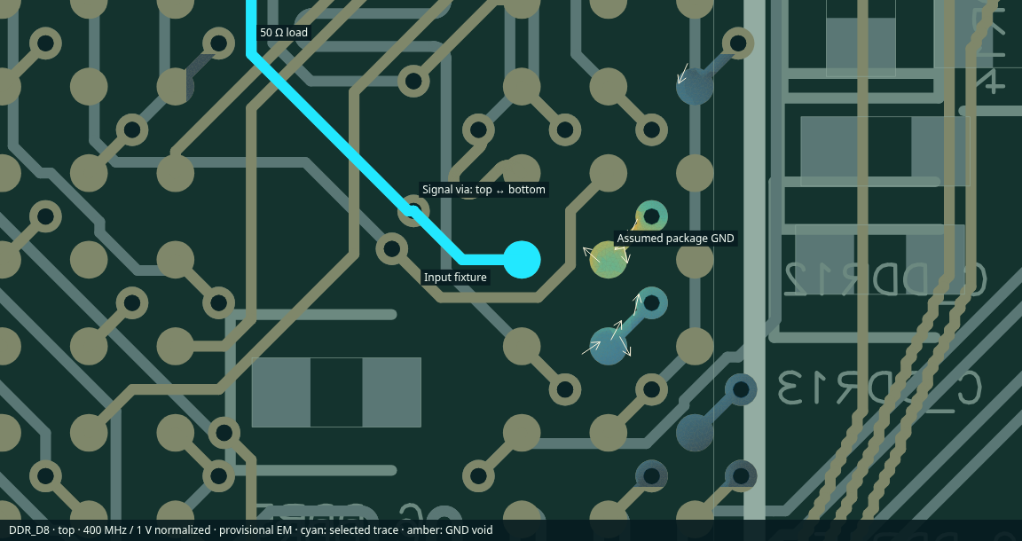 Open full-resolution image
Memory escape · 400 MHz · top/bottom signals · inner1/inner2 GND planes
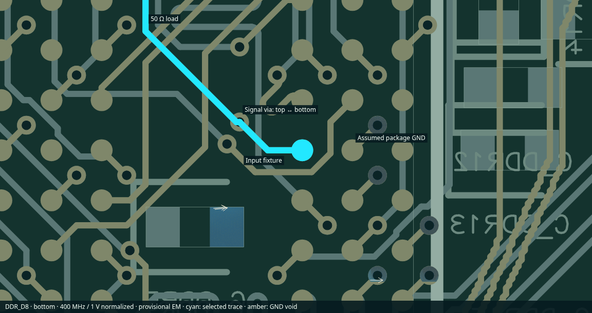
The input fixture joins the actual memory signal pad to its nearest exported package GND pad. It is a test fixture; package internals and the real driver are omitted. The cut bottom trace is terminated through a 50 Ω fixture to inner2 GND.
Drag to orbit · right-drag to pan · scroll to zoom. Hide individual copper layers to inspect the dogbones, hollow barrels and plane voids. Substrate and air are hidden.
Mesh provenance and countsChoose from 47 DDR connections. DDR_D8 and DDR_D13 have U1 processor EM overlays. DDR_D8 also has downstream and memory-side runs; other connections are PCB inspection only. Use PCB visibility and heat opacity to compare copper and return current.
Drag to pan; scroll to zoom. Labels stay the same size. Colors show surface-current phasor magnitude |K|. White arrows show instantaneous direction at phase 0°, which changes through the RF cycle.
Cyan: full selected DDR_D8 route. Amber: the two local EM domains.
 Open full-resolution image
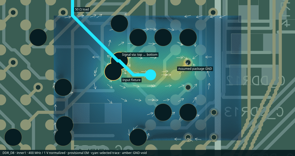 Open full-resolution image
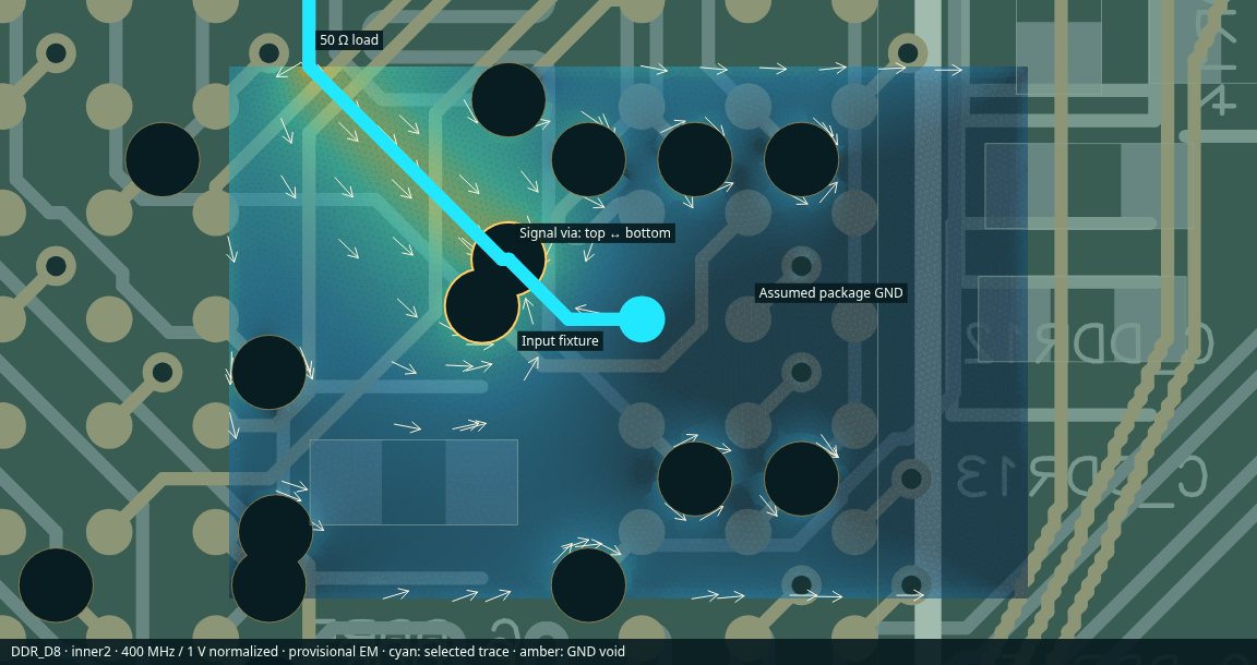 Open full-resolution image
 Open full-resolution image
First → second element order on the same mesh: input-current magnitude changed 14.7%; reactance changed 13.0%. This does not validate local-density peaks, crop extent or test fixtures. These are provisional normalized EM results.
| Solver | Palace v0.14.0 · 3D frequency-domain FEM Maxwell · order 2 |
|---|---|
| Excitation | 400 MHz · 1 V signal-to-GND normalized peak phasor · 50 Ω input reference and load |
| Stackup assumption | Top 1.6 / inner1 1.4 / inner2 0.2 / bottom 0 mm from bottom. Internal dielectric thicknesses are not supplied by the PCB export. |
| Materials | FR4 εr 4.3, tanδ 0.02 · copper 5.8×10⁷ S/m · copper foil 35 µm · via plating 25 µm |
| Mesh | 18,288 nodes · 57,797 tetrahedra · 0.1 mm minimum target · octagonal barrels |
| Domain | x [-1.5, 4.5], y [-25.5, -21.5] mm · 5 mm air padding · first-order absorbing boundary |
| Geometry | 1 selected signal via; 5 GND vias. Exported GND vias span top→inner1; signal vias span top↔bottom. The model follows those spans. Any inner1↔inner2 GND stitching through fabrication barrels, plated holes or copper outside these crops is omitted. This can strongly affect impedance; fabrication spans/stubs require confirmation. Other signal/power copper, package internals and decoupling are omitted. |
| Displayed ground faces | Inner1 upper face (toward top signal); inner2 lower face (toward bottom signal); outer GND faces. These are face currents, not sums across the two faces of a plane. |
SI phasor report · Solver configuration · Element-order comparison · Via currents · Source repository
PCB SHA-256: 80ef96cf94a1dac4f3d062f694fe71529a9a57f5a1dd6e8b1abdf92302968b13