PCB TRACE & RETURN-CURRENT INSPECTOR
Inspect DDR routing on the PCB
Drag to pan · scroll or use + / − to zoom · click a dogbone button for a close-up
Simulation parameters
Frequency: not specified — frequency-independent approximation. These experiments were not run at a DDR clock frequency or at 0 Hz. The model has no frequency input and does not calculate frequency-dependent impedance.
- Excitation
- 10 mA on one trace at a time
- Experiments
- 47 traces × 2 package-GND contact assumptions
- Ground-plane mesh
- 0.25 mm · 21,005 plane cells
- Assumed layer depths
- Top 0 / Inner 1 0.2 / Inner 2 1.4 / Bottom 1.6 mm
- Copper / via plating
- 35 µm copper / 25 µm radial plating
- Contact search radius
- 0.6 mm
- Region / boundary
- x: −23 to 11 mm; y: −39.5 to 3.5 mm · insulating crop boundary
- Solver
- Conservative graph projection · relative residual 10⁻⁸ · maximum 15,000 iterations
- Validation
- 94 converged cases · maximum current-balance error 8.18 × 10⁻¹¹ A
- Density display
- 0–0.15 A/mm² · bilinear interpolation for display
The exported GND pour is on the bottom layer. Inner-layer GND planes, frequency effects, package impedance and power-plane return through capacitors are not included.
Download all parameters (JSON)Trace comparisons and numerical details
| Trace | Processor: signal → return via | Memory: signal → return via |
|---|
Click a trace to inspect it on the PCB. These distances depend on the selected package-ground contact.
How to read the overlay and its limits
Cyan follows the selected signal’s actual routing across layers. The dim background combines PCB routing layers for orientation. Orange copper and arrows show the solved GND return current on the chosen heatmap layer. Orange via markers show transfer through GND via barrels. Purple marks the assumed package ground contact.
The dashed line is a straight-line distance measurement between two vias, not a simulated current path. The warm overlay shows horizontal GND density from 0 to 0.15 A/mm²; orange via markers identify current transfer. Inner-layer views have no horizontal GND pour in this export.
47 traces, two ground-contact cases per trace, all at an isolated 10 mA. This is the refined 0.25 mm-mesh approximation, with four times as many ground-plane cells, overlaid on board geometry. Density colors are interpolated between computed samples for display. It does not determine loop inductance or DDR timing margins. Package ground distribution and completeness of exported ground planes remain uncertain.
Earlier combined-current heatmaps
Colored copper shows GND return current. Gray DDR traces are routing context.
Horizontal density: 0–5 A/mm² · Via circles: 0–150 mA · Both scales saturate at their maximum.
Top
0 mm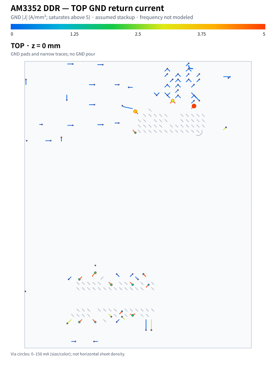
Return current in narrow GND connections and via barrels. No top GND pour was exported.
Inner 1
0.2 mm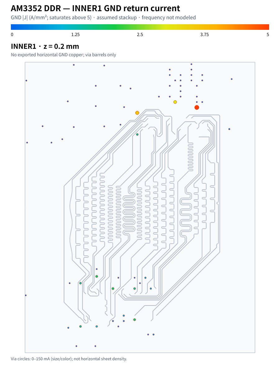
No horizontal GND copper was exported. Circles show current passing through GND via barrels.
Inner 2
1.4 mm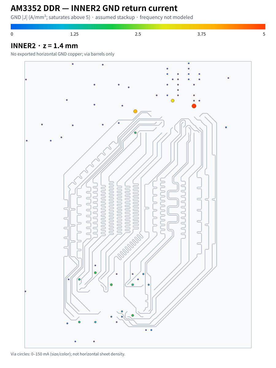
No horizontal GND copper was exported. Circles show current passing through GND via barrels.
Bottom
1.6 mm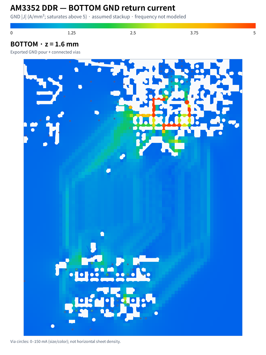
Return current spreads across the exported GND pour. White areas are gaps in that copper.
Simulation assumptions and validation
Original four-layer routes and 67 GND vias in the DDR region. The solve uses 40 single-ended lines at +10 mA and three balanced differential pairs at ±10 mA; reset is excluded. These are prescribed currents, not measured switching waveforms.
- Assumed layer depths
- 0 / 0.2 / 1.4 / 1.6 mm
- Copper / via plating
- 35 µm / 25 µm
- Ground mesh
- 0.5 mm pitch
- Maximum current-balance error
- 1.35 × 10⁻¹⁰ A
This connected multilayer image-current approximation omits frequency-dependent effects, package impedance and power-plane return through capacitors. The regional boundary is artificial. Current conservation checks the graph solve; it does not validate electromagnetic accuracy or DDR signal integrity.
The local extension passed 20 tests and TypeScript checks.