FREQUENCY-DOMAIN MAXWELL SOLVER · PALACE v0.14.0
400 MHz electromagnetic experiment
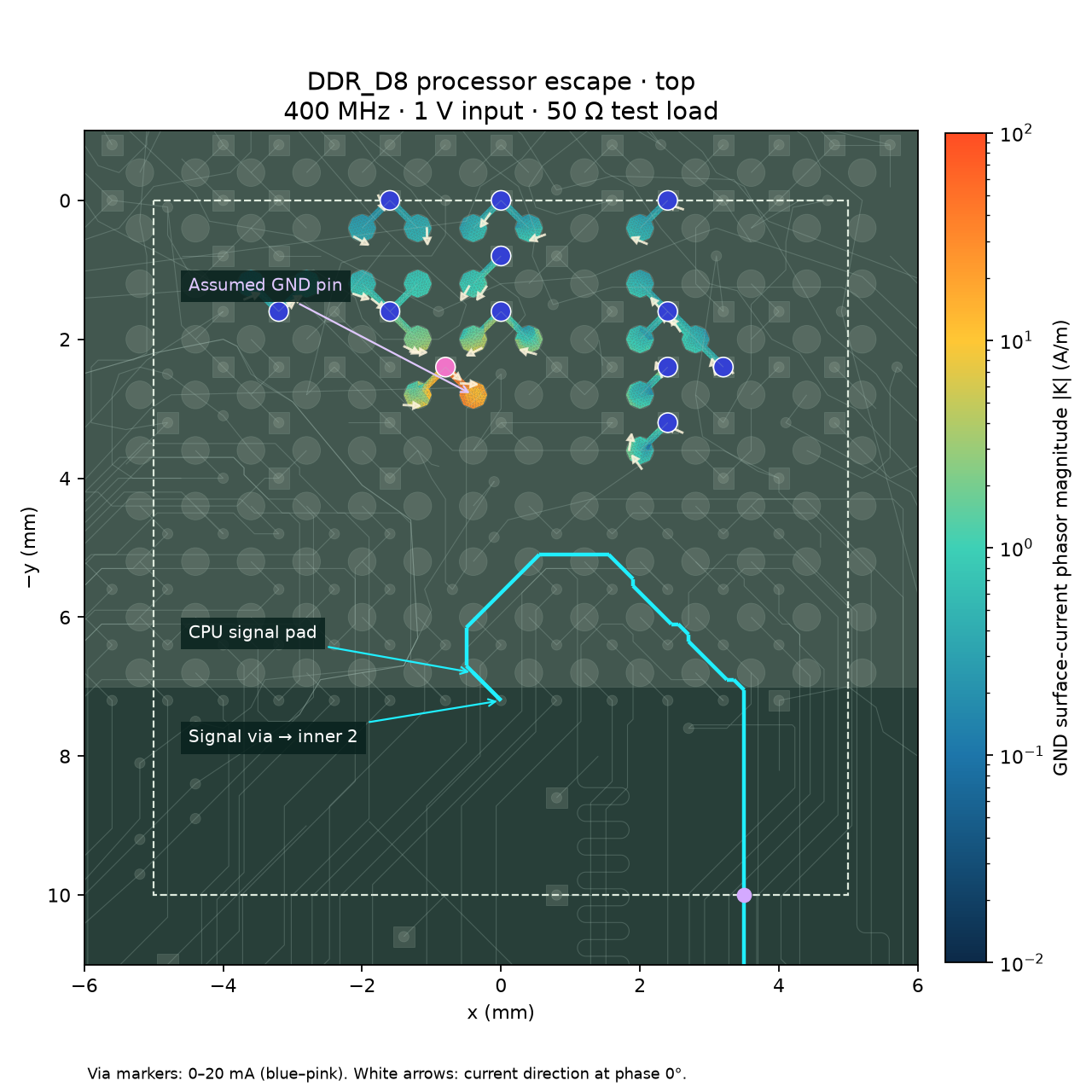
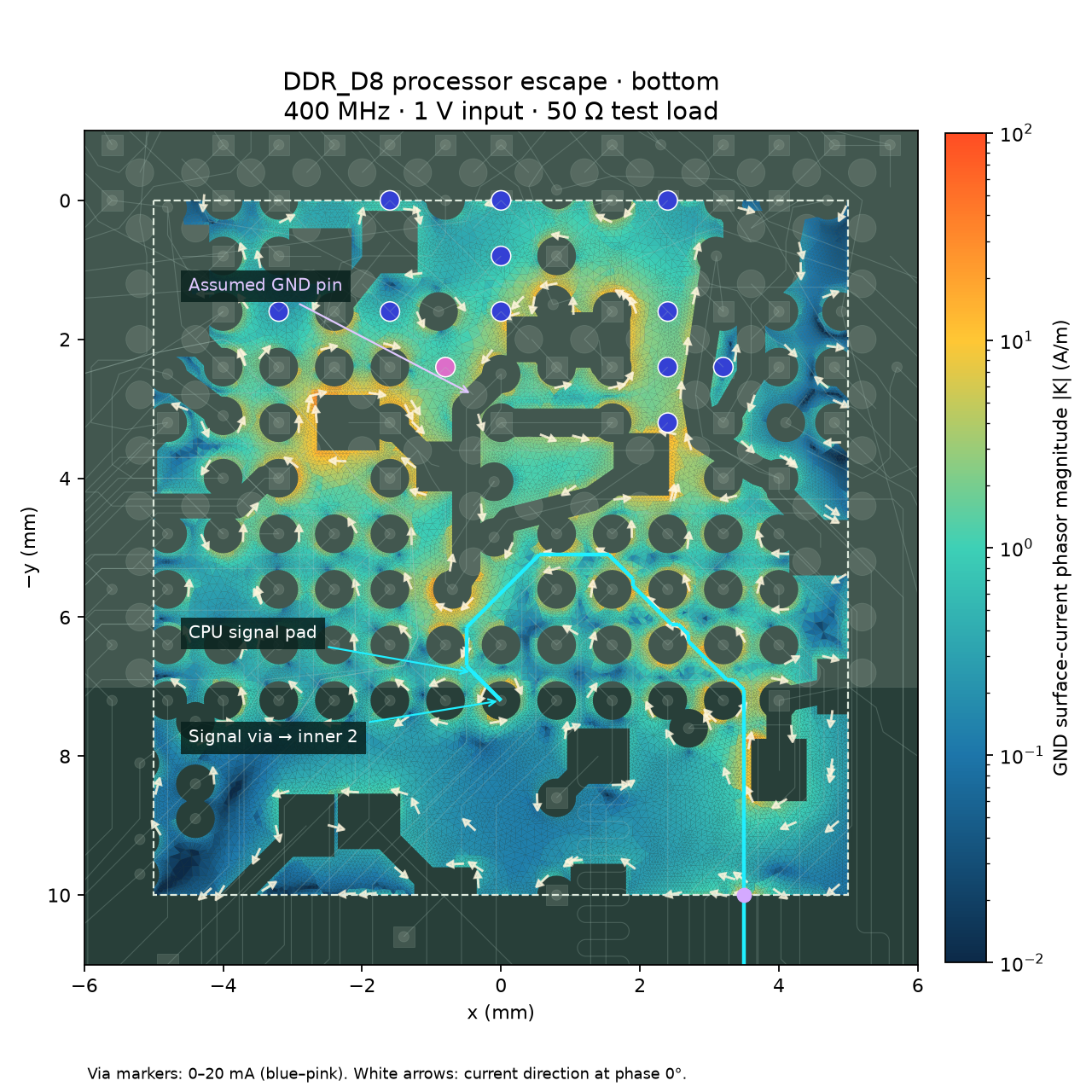
Processor dogbone of DDR_D8, with its actual routing and exported ground copper. Input terminal voltage normalized to 1 V; source reference and load are 50 Ω. Cyan highlights the signal. Color shows the magnitude of the solved GND surface-current phasor. White arrows show instantaneous direction at the input voltage peak (phase 0°); they are not streamlines.
First EM pilot — local densities and loop reactance are not yet numerically converged; fabrication accuracy remains unverified. This is a cropped escape experiment, with an assumed package-ground fixture and an artificial outgoing termination. It does not establish DDR timing margin or certify a return loop as good or bad.
Drag to pan · scroll to zoom · hover over a mesh triangle for its current density. Text stays outside the zooming PCB. The dashed box is the simulated region; the purple marker is the artificial load fixture.
0.01 → 100 A/m, logarithmic color scale; saturates at the endpoints. Values come from the FEM boundary mesh, converted to SI units.
Via markers use a separate scale: blue → pink, 0 → 20 mA of integrated barrel current. Hover for the value. Top/bottom barrel samples are 50 µm inside the substrate; inner samples are at their layer depth.
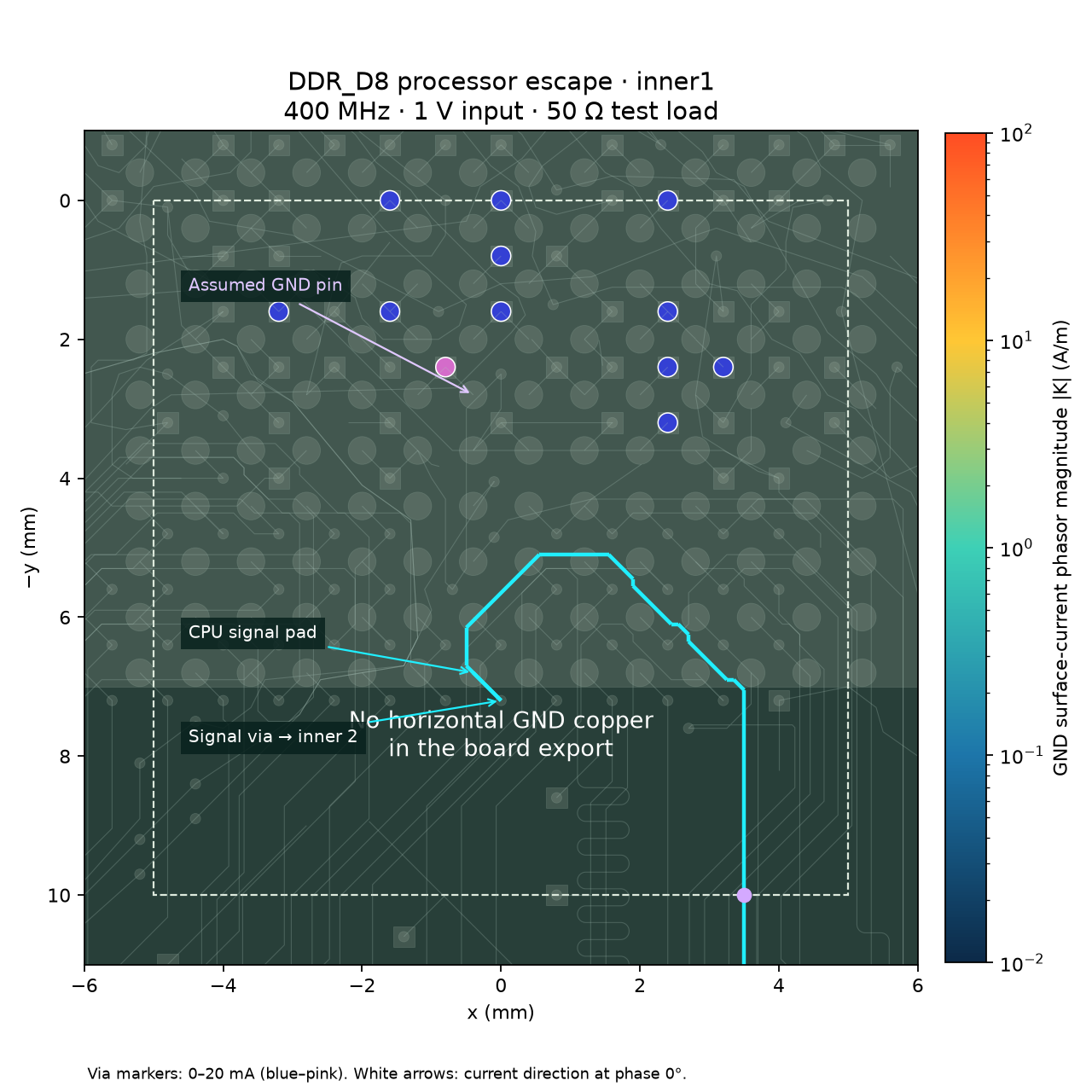
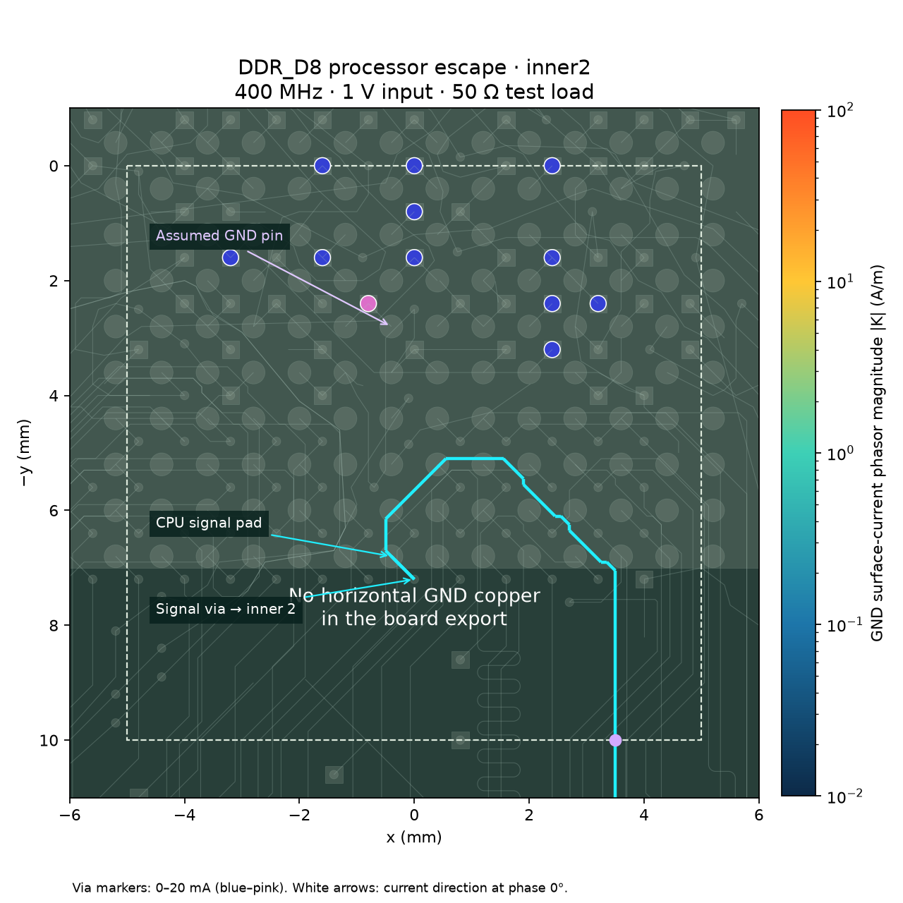
All four layer images
Simulation parameters and limits
3D frequency-domain finite-element Maxwell solve at 400 MHz. Copper is modeled with finite-conductivity surface impedance (σ = 5.8 × 10⁷ S/m); its skin depth is approximately 3.3 µm. The 35 µm copper interior is excluded from the field mesh. Surface current K is in A/m, rather than bulk current density in A/mm².
Uniform FR4: εᵣ = 4.3, loss tangent = 0.02. Four-layer depths, measured from the bottom: bottom 0, inner 2 0.2, inner 1 1.4, top 1.6 mm. Via plating is 25 µm; barrel cross-sections use eight facets. Planar copper polygons are simplified by at most 5 µm. Signal-via extent follows the exported top-to-inner-2 transition; through-hole stubs are not inferred.
Region: x −5 to 5 mm, y −10 to 0 mm. Twelve GND vias (including three on the crop boundary) and one signal via. Air padding 5 mm, first-order absorbing outer boundary. The source is a coplanar lumped fixture between the signal pad and the selected nearest package-ground pad. The load is a vertical 50 Ω fixture from the cut inner-2 trace to the bottom GND pour at (3.5, −10) mm. The source fixture spans a substantial distance and is an assumption, rather than a package model.
Other signal nets, power copper, package internals and decoupling capacitors are omitted. No inner-layer GND planes are present in the source export. These omissions, the artificial crop boundary, assumed stackup and unverified mesh/boundary convergence limit the physical accuracy of absolute values. This run establishes the EM workflow for the processor escape; it does not assess the complete trace or the memory escape.
Normalized port results and units · Palace configuration · Mesh details · Barrel-current integrals · Order-convergence check · Reproducible source